
 Add GTC Bharat on Google
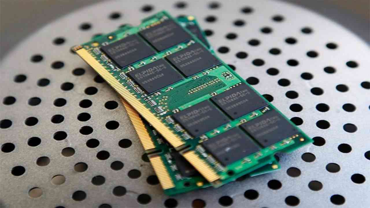
New Delhi, India: India's semiconductor opportunity is expanding beyond chip fabrication and packaging, with the country now focusing on building a complete ecosystem covering chip design, equipment, materials, advanced packaging, research and electronics products, YES Securities said in a report on the SEMICON India 2026 conclave.
The report said the next phase of India's semiconductor growth will depend on the country's ability to capture more value across the wider supply chain rather than focusing only on wafer fabrication. "The economic opportunity is potentially much larger in the ecosystem surrounding semiconductor manufacturing than in wafer fabrication alone," YES Securities said.
The report noted that the growing semiconductor ecosystem could create opportunities for suppliers, equipment manufacturers, engineering companies, packaging firms, materials producers and chip-design companies. The expansion is being supported by the government's Semicon 2.0 programme, which has an outlay of Rs 1,27,500 crore and focuses on six areas -- semiconductor design, machines and materials, new fabs, ATMP/OSAT, research and development, and talent.
The government has received investment commitments of around Rs 1 lakh crore under the programme, with these investments expected to materialise over the next two to three years, the report said. YES Securities said semiconductor demand is no longer the key constraint, with artificial intelligence, data centres, automobiles, industrial automation and communications emerging as major drivers of demand.
The focus, therefore, is shifting towards building sufficient supply-chain depth to enable India to capture a larger share of the growing semiconductor market. The report highlighted investments by global semiconductor companies as evidence of increasing localisation in the sector.
Applied Materials has announced a USD 5 billion investment over the next decade in India, including spending on research, supply-chain development and talent. Lam Research plans to invest around Rs 10,000 crore in a silicon-component manufacturing facility and expand its research and development activities.
Tata Electronics has also signed seven strategic agreements linked to its Dholera semiconductor fab. The agreements cover areas including fabrication, advanced packaging, materials, research, vendor development and workforce training, the report said. YES Securities identified semiconductor materials, specialised gases, equipment and precision manufacturing as some of the key gaps in India's semiconductor ecosystem.
The report said India does not need to achieve complete self-sufficiency across the semiconductor value chain. Instead, it should develop capabilities in strategically important areas while continuing to work with global suppliers. India's semiconductor design workforce remains a key strength, with government data cited in the report showing that the country accounts for around 20 per cent of the global chip-design workforce.
However, the report said the next challenge is to move from "designing for global companies" towards developing and owning semiconductor intellectual property, products and systems. "Execution and ecosystem depth" will determine how much economic value India captures as semiconductor demand expands, the report said. It added that advanced packaging, mature-node chips, precision manufacturing and product ownership could further expand India's role in the global semiconductor value chain. (ANI)